- 您现在的位置:买卖IC网 > Sheet目录2006 > LTC2630HSC6-LZ12#TRPBF (Linear Technology)IC DAC 12BIT R-R SC70-6
LTC2630
7
2630ff
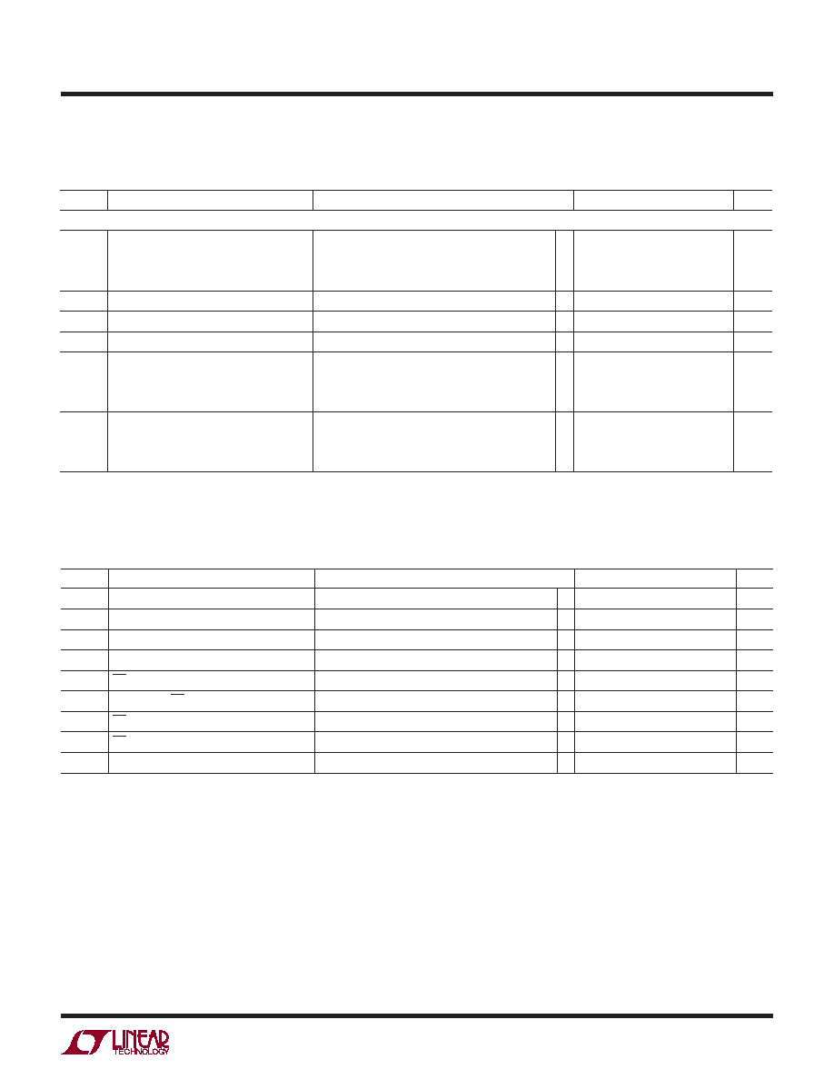
electrical characteristics The
l
denotes the specifications which apply over the full operating
temperature range, otherwise specifications are at TA = 25°C. VCC = 4.5V to 5.5V, VOUT unloaded unless otherwise specified.
LTC2630-HM12/-HM10/-HM8/-HZ12/-HZ10/-HZ8, LTC2630A-HM12/-HZ12 (VFS = 4.096V)
SYMBOL PARAMETER
CONDITIONS
MIN
TYP
MAX
UNITS
AC Performance
tS
Settling Time
VCC = 5V (Note 9)
±0.39% (±1LSB at 8 Bits)
±0.098% (±1LSB at 10 Bits)
±0.024% (±1LSB at 12 Bits)
3.7
4.4
4.8
s
Voltage Output Slew Rate
1.0
V/s
Capacitive Load Driving
500
pF
Glitch Impulse
At Mid-Scale Transition
2.4
nVs
en
Output Voltage Noise Density
At f = 1kHz, Supply as Reference
At f = 10kHz, Supply as Reference
At f = 1kHz, Internal Reference
At f = 10kHz, Internal Reference
140
130
210
200
nV/√Hz
Output Voltage Noise
0.1Hz to 10Hz, Supply as Reference
0.1Hz to 10Hz, Internal Reference
0.1Hz to 200kHz, Supply as Reference
0.1Hz to 200kHz, Internal Reference
20
650
750
VP-P
Note 1: Stresses beyond those listed under Absolute Maximum Ratings
may cause permanent damage to the device. Exposure to any Absolute
Maximum Rating condition for extended periods may affect device
reliability and lifetime.
Note 2: All voltages are with respect to GND.
Note 3: High temperatures degrade operating lifetimes. Operating lifetime
is derated at temperatures greater than 105°C.
Note 4: Linearity and monotonicity are defined from code kL to code 2N–1,
where N is the resolution and kL is given by kL = 0.016 (2N/ VFS), rounded
to the nearest whole code. For VFS = 2.5V and N = 12, kL = 26 and linearity
is defined from code 26 to code 4,095. For VFS = 4.096V and
N = 12, kL = 16 and linearity is defined from code 16 to code 4,095.
Note 5: Inferred from measurement at code 16 (LTC2630-12), code 4
(LTC2630-10) or code 1 (LTC2630-8).
Note 6: This IC includes current limiting that is intended to protect the
device during momentary overload conditions. Junction temperature can
exceed the rated maximum during current limiting. Continuous operation
above the specified maximum operating junction temperature may impair
device reliability.
Note 7: Digital inputs at 0V or VCC.
Note 8: Guaranteed by design and not production tested.
Note 9: Internal Reference mode. DAC is stepped 1/4 scale to 3/4 scale
and 3/4 scale to 1/4 scale. Load is 2k
W in parallel with 100pF to GND.
Note 10: Temperature coefficient is calculated by dividing the maximum
change in output voltage by the specified temperature range.
timing characteristics The
l
denotes the specifications which apply over the full operating temperature
range, otherwise specifications are at TA = 25°C. VCC = 4.5V to 5.5V. (See Figure 1) (Note 8).
LTC2630-HM12/-HM10/-HM8/-HZ12/-HZ10/-HZ8, LTC2630A-HM12/-HZ12 (VFS = 4.096V)
SYMBOL PARAMETER
CONDITIONS
MIN
TYP
MAX
UNITS
t1
SDI Valid to SCK Setup
l
4
ns
t2
SDI Valid to SCK Hold
l
4
ns
t3
SCK High Time
l
9
ns
t4
SCK Low Time
l
9
ns
t5
CS/LD Pulse width
l
10
ns
t6
SCK High to CS/LD High
l
7
ns
t7
CS/LD Low to SCK High
l
7
ns
t10
CS/LD High to SCK Positive Edge
l
7
ns
SCK Frequency
50% Duty Cycle
l
50
MHz
发布紧急采购,3分钟左右您将得到回复。
相关PDF资料
LTC2642IDD-16#PBF
IC DAC 16BIT VOUT 10-DFN
LTC2704IGW-16#PBF
IC DAC 16BIT QUAD VOUT 44-SSOP
LTC2751AIUHF-16#PBF
IC DAC 16BIT CUR OUT 38-QFN
LTC2752ACLX#PBF
IC DAC 16BIT DUAL CUR OUT 48LQFP
LTC2753AIUK-16#TRPBF
IC DAC 16BIT DUAL 48-QFN
LTC2754AIUKG-16#PBF
IC DAC 16BIT QUAD IOUT 52-QFN
LTC2755AIUP-16#PBF
IC DAC 16BIT CUR OUT 64-QFN
LTC2757ACLX#PBF
IC DAC 18BIT PAR 48LQFP
相关代理商/技术参数
LTC2630HSC6-LZ8#PBF
制造商:Linear Technology 功能描述:8BIT DAC R/R INT REF SMD SC70-6 制造商:Linear Technology 功能描述:8BIT DAC R/R, INT REF, SMD, SC70-6
LTC2630HSC6-LZ8#TRMPBF
功能描述:IC DAC 8BIT R-R SC70-6 RoHS:是 类别:集成电路 (IC) >> 数据采集 - 数模转换器 系列:- 产品培训模块:Lead (SnPb) Finish for COTS
Obsolescence Mitigation Program 标准包装:58 系列:- 设置时间:6µs 位数:8 数据接口:并联 转换器数目:4 电压电源:双 ± 功率耗散(最大):640mW 工作温度:-40°C ~ 85°C 安装类型:表面贴装 封装/外壳:24-SSOP(0.209",5.30mm 宽) 供应商设备封装:24-SSOP 包装:管件 输出数目和类型:4 电压,单极;4 电压,双极 采样率(每秒):*
LTC2630HSC6-LZ8#TRPBF
功能描述:IC DAC 8BIT R-R SC70-6 RoHS:是 类别:集成电路 (IC) >> 数据采集 - 数模转换器 系列:- 产品培训模块:Data Converter Fundamentals
DAC Architectures 设计资源:Unipolar, Precision DC Digital-to-Analog Conversion using AD5450/1/2/3 8-14-Bit DACs (CN0052)
Precision, Bipolar, Configuration for AD5450/1/2/3 8-14bit Multiplying DACs (CN0053)
AC Signal Processing Using AD5450/1/2/3 Current Output DACs (CN0054)
Programmable Gain Element Using AD5450/1/2/3 Current Output DAC Family (CN0055)
Single Supply Low Noise LED Current Source Driver Using a Current Output DAC in the Reverse Mode (CN0139) 标准包装:10,000 系列:- 设置时间:- 位数:12 数据接口:DSP,MICROWIRE?,QSPI?,串行,SPI? 转换器数目:1 电压电源:单电源 功率耗散(最大):- 工作温度:-40°C ~ 125°C 安装类型:表面贴装 封装/外壳:SOT-23-8 薄型,TSOT-23-8 供应商设备封装:TSOT-23-8 包装:带卷 (TR) 输出数目和类型:1 电流,单极;1 电流,双极 采样率(每秒):2.7M
LTC2630ISC6-HM10#TRMPBF
功能描述:IC DAC 10BIT R-R SC70-6 RoHS:是 类别:集成电路 (IC) >> 数据采集 - 数模转换器 系列:- 产品培训模块:Lead (SnPb) Finish for COTS
Obsolescence Mitigation Program 标准包装:58 系列:- 设置时间:6µs 位数:8 数据接口:并联 转换器数目:4 电压电源:双 ± 功率耗散(最大):640mW 工作温度:-40°C ~ 85°C 安装类型:表面贴装 封装/外壳:24-SSOP(0.209",5.30mm 宽) 供应商设备封装:24-SSOP 包装:管件 输出数目和类型:4 电压,单极;4 电压,双极 采样率(每秒):*
LTC2630ISC6-HM10#TRPBF
功能描述:IC DAC 10BIT R-R SC70-6 RoHS:是 类别:集成电路 (IC) >> 数据采集 - 数模转换器 系列:- 产品培训模块:Data Converter Fundamentals
DAC Architectures 设计资源:Unipolar, Precision DC Digital-to-Analog Conversion using AD5450/1/2/3 8-14-Bit DACs (CN0052)
Precision, Bipolar, Configuration for AD5450/1/2/3 8-14bit Multiplying DACs (CN0053)
AC Signal Processing Using AD5450/1/2/3 Current Output DACs (CN0054)
Programmable Gain Element Using AD5450/1/2/3 Current Output DAC Family (CN0055)
Single Supply Low Noise LED Current Source Driver Using a Current Output DAC in the Reverse Mode (CN0139) 标准包装:10,000 系列:- 设置时间:- 位数:12 数据接口:DSP,MICROWIRE?,QSPI?,串行,SPI? 转换器数目:1 电压电源:单电源 功率耗散(最大):- 工作温度:-40°C ~ 125°C 安装类型:表面贴装 封装/外壳:SOT-23-8 薄型,TSOT-23-8 供应商设备封装:TSOT-23-8 包装:带卷 (TR) 输出数目和类型:1 电流,单极;1 电流,双极 采样率(每秒):2.7M
LTC2630ISC6-HM12#PBF
制造商:Linear Technology 功能描述:IC 12BIT DAC R/R INT REF SC70-6 制造商:Linear Technology 功能描述:MS-DAC/Industrial, Cut Tape 12-bit Vout DAC SC70
LTC2630ISC6-HM12#TRMPBF
功能描述:IC DAC 12BIT R-R SC70-6 RoHS:是 类别:集成电路 (IC) >> 数据采集 - 数模转换器 系列:- 产品培训模块:Lead (SnPb) Finish for COTS
Obsolescence Mitigation Program 标准包装:58 系列:- 设置时间:6µs 位数:8 数据接口:并联 转换器数目:4 电压电源:双 ± 功率耗散(最大):640mW 工作温度:-40°C ~ 85°C 安装类型:表面贴装 封装/外壳:24-SSOP(0.209",5.30mm 宽) 供应商设备封装:24-SSOP 包装:管件 输出数目和类型:4 电压,单极;4 电压,双极 采样率(每秒):*
LTC2630ISC6-HM12#TRPBF
功能描述:IC DAC 12BIT R-R SC70-6 RoHS:是 类别:集成电路 (IC) >> 数据采集 - 数模转换器 系列:- 产品培训模块:Data Converter Fundamentals
DAC Architectures 设计资源:Unipolar, Precision DC Digital-to-Analog Conversion using AD5450/1/2/3 8-14-Bit DACs (CN0052)
Precision, Bipolar, Configuration for AD5450/1/2/3 8-14bit Multiplying DACs (CN0053)
AC Signal Processing Using AD5450/1/2/3 Current Output DACs (CN0054)
Programmable Gain Element Using AD5450/1/2/3 Current Output DAC Family (CN0055)
Single Supply Low Noise LED Current Source Driver Using a Current Output DAC in the Reverse Mode (CN0139) 标准包装:10,000 系列:- 设置时间:- 位数:12 数据接口:DSP,MICROWIRE?,QSPI?,串行,SPI? 转换器数目:1 电压电源:单电源 功率耗散(最大):- 工作温度:-40°C ~ 125°C 安装类型:表面贴装 封装/外壳:SOT-23-8 薄型,TSOT-23-8 供应商设备封装:TSOT-23-8 包装:带卷 (TR) 输出数目和类型:1 电流,单极;1 电流,双极 采样率(每秒):2.7M